Expanded by around 10 15 % to incorporate recent developments in the field, the new edition of this highly successful textbook is unique in its tutorial presentation of the physical concepts and experimental approaches that lie at the heart of nanotechnology.
A completely new section has been added on graphene, covering physical and electrical properties, synthesis and applications, as well as discussions of computer logic devices, silicon technology, and potential applications in photovoltaics. There are updates and corrections to every chapter, including the references, while the modern–day examples are chosen to represent important concepts and research
tools. Mathematical derivations are boxed in to be consulted as desired by those readers with a pertinent interest.
Well illustrated, including explanatory diagrams to assist in the understanding of scientific principles, this is a self–contained text for upper–level undergraduate engineering or science students looking for a concise, easy–to–read introduction to this fascinating field of research.
A free solutions manual is available for lecturers.
Table of Contents
Preface XV
Glossary of abbreviations XVII
1 Introduction 1
1.1 Nanometers, Micrometers, and Millimeters 3
1.1.1 Plenty of Room at the Bottom 4
1.1.2 Scaling the Xylophone 4
1.1.3 Reliability of Concepts and Approximate Parameter Values Down to About L = 10 nm (100 Atoms) 5
1.1.4 Nanophysics Built into the Properties of Bulk Matter 6
1.2 Moore s Law 7
1.3 Esaki s Quantum Tunneling Diode 9
1.4 QDs of Many Colors 10
1.5 GMR and TMR 100 1000 Gb Hard Drive Read Heads 11
1.6 Accelerometers in Your Car 14
1.7 Nanopore Filters 15
1.8 Nanoscale Elements in Traditional Technologies 15
References 16
2 Systematics of Making Things Smaller, Pre–quantum 17
2.1 Mechanical Frequencies Increase in Small Systems 17
2.2 Scaling Relations Illustrated by a Simple Harmonic Oscillator 20
2.3 Scaling Relations Illustrated by Simple Circuit Elements 21
2.4 Thermal Time Constants and Temperature Differences Decrease 22
2.5 Viscous Forces Become Dominant for Small Particles in Fluid Media 22
2.6 Frictional Forces Can Disappear in Symmetric Molecular Scale Systems 24
References 26
3 What Are Limits to Smallness? 27
3.1 Particle (Quantum) Nature of Matter: Photons, Electrons, Atoms, and Molecules 27
3.2 Biological Examples of Nanomotors and Nanodevices 28
3.2.1 Linear Spring Motors 29
3.2.2 Linear Engines on Tracks 30
3.2.3 Rotary Motors 33
3.2.4 Ion Channels, the Nanotransistors of Biology 36
3.2.4.1 Ca++–Gated Potassium Channel 37
3.2.4.2 Voltage–Gated Potassium Channel 37
3.3 How Small Can You Make it? 38
3.3.1 What Are the Methods for Making Small Objects? 39
3.3.2 How Can You SeeWhat YouWant to Make? 39
3.3.3 How Can You Connect it to the OutsideWorld? 42
3.3.4 If You Cannot See it or Connect to it, Can You Make it Self–Assemble and Work on its Own? 42
3.3.5 Approaches to Assembly of Small Three–Dimensional Objects 42
3.3.5.1 VariableThickness Electroplating 43
3.3.5.2 Lithography onto Curved Surfaces 43
3.3.5.3 Optical Tweezers 43
3.3.5.4 Arrays of Optical Traps 45
3.3.6 Use of DNA Strands in Guiding Self–Assembly of Nanometer–Sized Structures 46
References 48
4 Quantum Nature of the Nanoworld 51
4.1 Bohr s Model of Nuclear Atom 52
4.1.1 Quantization of Angular Momentum 52
4.1.2 Extensions of Bohr s Model 53
4.2 Particle Wave Nature of Light and Matter, DeBroglie Formulas = h¨Mp, E = h 54
4.3 Wavefunction for Electron, Probability Density , Traveling and StandingWaves 55
4.4 Maxwell s Equations; E and B asWavefunctions for Photons, Optical FiberModes 59
4.5 The Heisenberg Uncertainty Principle 60
4.6 Schrodinger Equation, Quantum States and Energies, Barrier Tunneling 61
4.6.1 Schrodinger Equations in One Dimension 62
4.6.1.1 Time–Dependent Equation 62
4.6.1.2 Time–Independent Equation 63
4.6.2 The Trapped Particle in One Dimension 63
4.6.2.1 Linear Combinations of Solutions 64
4.6.2.2 Expectation Values 64
4.6.2.3 Two–ParticleWavefunction 65
4.6.3 Reflection and Tunneling at a Potential Step 65
4.6.3.1 Case 1: E > Uo 66
4.6.3.2 Case 2: E
4.6.4 Penetration of a Barrier, Escape Time from a Well, Resonant Tunneling Diode 67
4.6.5 Trapped Particles in Two andThree Dimensions: Quantum Dot 68
4.6.5.1 Electrons Trapped in a 2D Box 69
4.6.5.2 Electrons in a 3D Quantum Dot 70
4.6.6 2D Bands and QuantumWires 71
4.6.6.1 2D Band 71
4.6.6.2 QuantumWire 71
4.6.7 The Simple Harmonic Oscillator 72
4.6.8 Schrodinger Equation in Spherical Polar Coordinates 73
4.7 The Hydrogen Atom, One–Electron Atoms, Excitons 74
4.7.1 Magnetic Moments 78
4.7.2 Magnetization and Magnetic Susceptibility 79
4.7.3 Positronium and Excitons 80
4.8 Fermions, Bosons, and Occupation Rules 81
References 81
5 Quantum Consequences for the Macroworld 83
5.1 Chemical Table of the Elements 83
5.2 Nanosymmetry, Diatoms, and Ferromagnets 84
5.2.1 Indistinguishable Particles and Their Exchange 84
5.2.1.1 Fermions 85
5.2.1.2 Bosons 85
5.2.1.3 Orbital and Spin Components ofWavefunctions 85
5.2.2 The Hydrogen Molecule, Dihydrogen:The Covalent Bond 86
5.2.2.1 Covalent Bonding and Covalent AntiBonding, Purely Nanophysical Effects 87
5.2.2.2 Ferromagnetism, a Purely Nanophysical Effect 87
5.3 More Purely Nanophysical Forces: van derWaals, Casimir, and Hydrogen Bonding 88
5.3.1 The Polar and van derWaals Fluctuation Forces 89
5.3.1.1 Electric Polarizability of Neutral Atoms and Molecules 89
5.3.1.2 Dipolar Fluctuations of Neutral and Symmetric Atoms 90
5.3.2 The Casimir Force 92
5.3.3 The Hydrogen Bond 96
5.4 Metals as Boxes of Free Electrons: Fermi Level, DOS, Dimensionality 97
5.4.1 Electronic Conduction, Resistivity, Mean Free Path, Hall Effect, Magnetoresistance 100
5.5 Periodic Structures (e.g., Si, GaAs, InSb, Cu): Kronig Penney Model for Electron Bands and Gaps 101
5.6 Electron Bands and Conduction in Semiconductors and Insulators; Localization versus Delocalization 107
5.7 Hydrogenic Donors and Acceptors 110
5.7.1 Carrier Concentrations in Semiconductors, Metallic Doping 112
5.7.2 PN Junction, Electrical Diode I(V) Characteristic, Injection Laser 116
5.7.2.1 Radiative Recombination and Emission of Light 117
5.7.2.2 PN Junction Injection Laser 118
5.7.2.3 Increasing Radiative Efficiency 119
5.7.2.4 Single–Nanowire Electrically Driven Laser 119
5.8 More about Ferromagnetism, the Nanophysical Basis of Disk Memory 121
5.9 Surfaces are Different; Schottky Barrier Thickness W = [2 o VB¨MeND]1¨M2 124
5.10 Ferroelectrics, Piezoelectrics, and Pyroelectrics: Recent Applications to Advancing Nanotechnology 126
5.10.1 Piezoelectric Materials 126
5.10.2 Ultrasonic Initiation of Bubbles, by a Negative Pressure 127
5.10.3 Ferroelectrics and Pyroelectrics 127
5.10.4 A Nanotechnological (Pyroelectric) Compact Source of Neutrons 128
5.10.5 Electric Field Ionization of Deuterium (Hydrogen) 129
5.10.6 An Unexpected High–Temperature Nanoenvironment 131
5.10.7 Collapse of Ultrasonically Produced Bubbles in Dense Liquids 131
References 134
6 Self–Assembled Nanostructures in Nature and Industry 137
6.1 Carbon Atom 12
6C 1s2 2p4 (0.07 nm) 138
6.2 Methane (CH4), Ethane (C2H6), and Octane (C8H18) 139
6.3 Ethylene (C2H4), Benzene (C6H6), and Acetylene (C2H2) 140
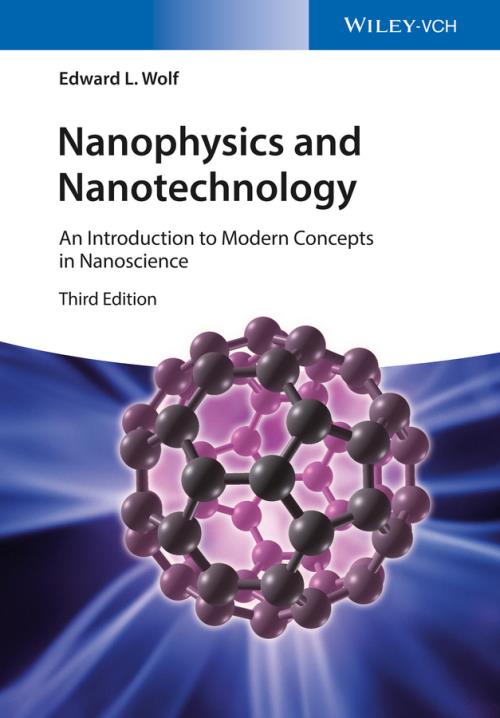
6.4 C60 Buckyball ( 0.5 nm) 140
6.5 C Nanotube ( 0.5 nm) 141
6.5.1 Si Nanowire ( 5 nm) 144
6.6 InAs Quantum Dot ( 5 nm) 145
6.7 AgBr Nanocrystal (0.1 2 m) 146
6.8 Fe3O4 Magnetite and Fe3S4 Greigite Nanoparticles in Magnetotactic Bacteria 147
6.9 Self–Assembled Monolayers on Au and Other Smooth Surfaces 149
References 151
7 Physics–Based Experimental Approaches to Nanofabrication and Nanotechnology 153
7.1 Silicon Technology:The INTEL–IBM Approach to Nanotechnology 154
7.1.1 Patterning, Masks, and Photolithography 154
7.1.1.1 Patterning Deposition Masks 154
7.1.1.2 Masking Layers to Limit Etching 155
7.1.2 Etching Silicon 155
7.1.2.1 Wet Etches 155
7.1.2.2 Dry Etches 156
7.1.3 Defining Highly Conducting Electrode Regions 156
7.1.4 Methods of Deposition of Metal and Insulating Films 156
7.1.4.1 Evaporation 156
7.1.4.2 Sputtering 157
7.1.4.3 Chemical Vapor Deposition 157
7.1.4.4 Laser Ablation 157
7.1.4.5 Molecular Beam Epitaxy 157
7.1.4.6 Ion Implantation 158
7.2 Lateral Resolution (Linewidths) Limited byWavelength of Light, Now 65 nm 158
7.2.1 Optical and X–Ray Lithography 158
7.2.2 Electron–Beam Lithography 159
7.3 Sacrificial Layers, Suspended Bridges, Single–Electron Transistors 160
7.4 What Is the Future of Silicon Computer Technology? 162
7.5 Heat Dissipation and the RSFQ Technology 163
7.6 Scanning Probe (Machine) Methods: One Atom at a Time 167
7.7 STM as Prototype Molecular Assembler 169
7.7.1 Moving Au Atoms, Making Surface Molecules 169
7.7.2 Assembling Organic Molecules with an STM 172
7.8 Atomic Force Microscope Arrays 173
7.8.1 Cantilever Arrays by Photolithography 173
7.8.2 Nanofabrication with an AFM 174
7.8.3 Imaging a Single Electron Spin by a Magnetic Resonance AFM 175
7.9 Fundamental Questions: Rates, Accuracy, and More 177
7.10 Nanophotonics and Nanoplasmonics 178
References 181
8 Quantum Technologies Based on Magnetism, Electron and Nuclear Spin, and Superconductivity 183
8.1 Spin as an Element of Quantum Computing 183
8.2 The Stern Gerlach Experiment: Observation of Spin–1¨M2; Angular Momentum of the Electron 186
8.3 Two Nuclear Spin Effects: MRI (Magnetic Resonance Imaging) and the 21.1 cm Line 187
8.4 Electron Spin 1¨M2; as a Qubit for a Quantum Computer: Quantum Superposition, Coherence 190
8.5 Hard and Soft Ferromagnets 193
8.6 The Origins of GMR (Giant Magnetoresistance): Spin–Dependent Scattering of Electrons 194
8.7 The GMR Spin Valve, a Nanophysical Magnetoresistance Sensor 197
8.8 The Tunnel Valve, a Better (TMR) Nanophysical Magnetic Field Sensor 198
8.9 Magnetic Random Access Memory 200
8.9.1 Magnetic Tunnel Junction MRAM Arrays 200
8.9.2 Hybrid Ferromagnet Semiconductor Nonvolatile Hall Effect Gate Devices 200
8.10 Spin Injection: The Johnson Silsbee Effect 203
8.10.1 Apparent Spin Injection from a Ferromagnet into a Carbon Nanotube 203
8.11 Magnetic Logic Devices: A Majority Universal Logic Gate 203
8.12 Superconductors and the Superconducting (Magnetic) Flux Quantum 206
8.13 Josephson Effect and the Superconducting Quantum Interference Device (SQUID) 211
8.14 Superconducting (RSFQ) Logic/Memory Computer Elements 214
8.14.1 The Single Flux Quantum Voltage Pulse 215
8.14.2 Analog–to–Digital Conversion (ADC) Using RSFQ Logic 217
References 217
9 Silicon Nanoelectronics and Beyond 219
9.1 Electron Interference Devices with Coherent Electrons 220
9.1.1 Ballistic Electron Transport in Stubbed Quantum Waveguides: Experiment and Theory 222
9.1.2 Well–Defined Quantum Interference Effects in Carbon Nanotubes 223
9.2 Carbon Nanotube Sensors and Dense Nonvolatile Random Access Memories 226
9.2.1 A Carbon Nanotube Sensor of Polar Molecules, Making Use of the Inherently Large Electric Fields 227
9.2.2 Carbon Nanotube Cross–Bar Arrays for Ultradense Ultrafast Nonvolatile Random Access Memory 228
9.3 Resonant Tunneling Diodes, Tunneling Hot Electron Transistors 232
9.4 Double–Well Potential Charge Qubits 233
9.4.1 Silicon–Based Quantum Computer Qubits 238
9.5 Single Electron Transistors 239
9.5.1 RFSET, a Useful Proven Research Tool 242
9.5.2 Readout of the Charge Qubit, with Subelectron Charge Resolution 242
9.5.3 A Comparison of SET and RTD Behaviors 244
9.6 Experimental Approaches to the Double–Well Charge Qubit 245
9.6.1 Coupling of Two–Charge Qubits in a Solid–State (Superconducting) Context 249
9.7 Ion Trap on a GaAs Chip, Pointing to a New Qubit 253
9.8 Quantum Computing by Quantum Annealing with Artificial Spins 254
References 255
10 Nanophysics and Nanotechnology of Graphene 257
10.1 Graphene: Record–Breaking Physical and Electrical Properties 257
10.2 Consequences of One–AtomThickness: Softness and Adherence 258
10.3 Impermeability of Single–Layer Graphene 258
10.4 Synthesis by Chemical Vapor Deposition and Direct Reaction 260
10.5 Application to Flexible, Conducting, and Transparent Electrodes 262
10.6 Potential Application to Computer Logic Devices, Extending Moore s Law 264
10.7 Applications of Graphene within Silicon Technology 266
References 268
11 Looking into the Future 271
11.1 Drexler s Mechanical (Molecular) Axle and Bearing 271
11.1.1 Smalley s Refutation of Machine Assembly 272
11.1.2 van derWaals Forces for Frictionless Bearings? 274
11.2 The Concept of the Molecular Assembler is Flawed 275
11.3 Could Molecular Machines Revolutionize Technology or Even Self–Replicate toThreaten Terrestrial Life? 276
11.4 The Prospect of Radical Abundance by a Breakthrough in Nanoengineering 277
11.5 What about Genetic Engineering and Robotics? 278
11.6 Possible Social and Ethical Implications of Biotechnology and Synthetic Biology 281
11.7 Is there a Posthuman Future as Envisioned by Fukuyama? 282
References 284
Some Useful Constants 285
Exercises 287
Index 297


