While creating integrated circuits, a thin wafer is a slice of semiconductor material. One of the main drivers of a thin wafer market's expansion is the rising demand for semiconductor devices in sectors like telecommunications, consumer electronics, and automotive.
Wafer, also known as a slice or a substrate, is a thin semiconductor slice used in electronics for the production of solar cells and integrated circuits made of crystalline silicon (c-Si). The wafer, which serves as the foundation for those devices, is built inside of and on top. It undergoes numerous microfabrication techniques, such as photolithographic patterning, electrodeposition, doping, etching, and thin-film deposition of various materials. The individual microcircuits are separated by wafer dicing, and they are subsequently assembled into an integrated circuit.
Wafers are made of material that is extremely pure, almost defect-free and has a purity of 99.9999999percentage points (9N) or higher. The C zochralski method, developed by Polish chemist Jan Czochralski, is one method for producing crystalline wafers. Pulling a seed crystal from a melt creates a boule, a cylindrical ingot of a high-purity monocrystalline semiconductor like silicon or germanium. The molten intrinsic material can be doped to create an extrinsic semiconductor of the n-type or p-type by adding donor impurity atoms in exact proportions, such as boron or phosphorus in the case of silicon.
The boule is then cut into wafer-shaped pieces using a wafer saw (a sort of wire saw), machined to increase flatness, chemically erased to remove machining-related crystal damage, and polished to finish. Photovoltaic wafers range in size from 100 to 200 mm square and range in thickness from 100 to 500 m. Electronics employ wafers with diameters ranging from 100 to 450 mm. The largest manufactured wafers are 450 mm in diameter, although they are not yet in widespread use.
COVID-19 Impact Analysis
The thin wafer industry includes producers of Tier 1 and Tier 2 with manufacturing facilities dispersed across numerous nations. These companies produce thin wafers that are utilized in a variety of end markets, including electronics, automobiles, medical, and a few more. Covid-19 had an impact on both enterprises in the aforementioned sectors as well as thin wafer industry players' operations. The market for MEMS products from the automotive and electronic goods sectors is also anticipated to decrease. The present COVID-19 pandemic has harmed the market for thin wafer processing and dicing equipment, causing a sizable output slowdown as manufacturing activities are momentarily suspended throughout key industrial centers.Market Growth Factors
Smaller Electrical Device Sizes High 5g Technology Adoption
Companies all around the world are switching to 5G connectivity to boost operational effectiveness and increase transaction volumes. Additionally, 5G networks can give substantially faster speeds and shorter download times, making them suitable for use in sectors like automotive and smart city development. GaN-based thin wafers, which have the potential to achieve power-added efficiencies (PAE) of 50% or more, are expected to gain popularity. Additionally, it is projected that 5G technology would be widely used in fields like AI, driverless vehicles, and augmented reality. Additionally, the Dutch chipmaker NXP opened a GaN 5G chip manufacturing facility in Arizona intending to enhance 5G communications equipment. This is propelling market expansion.Increasing IoT And AI Usage In The Automotive Sector
The introduction of Industry 4.0 and new technologies like IoT and AI in the automobile industry will have a big impact on the expansion of the thin wafer market. The rising need for car connectivity will spur new industry advancements. Additionally, the relevance of linked cars is expanding as a result of current trends like touch-free human-machine interfaces, which are transforming the automotive industry. One of the main drivers of future IoT connection growth is the integration of IoT in vehicle safety and communication technologies. The advent of new technologies including adaptive cruise control, intelligent parking assistance systems, and advanced driver assistance systems (ADAS) will further spur market expansion.Marketing Restraining Factor:
The Maintenance Of Narrow Wafer Efficiency Is A Critical Issue
Efficiency is the major problem businesses are currently having while implementing thin wafers. A narrow wafer has poor capability for long-wavelength light absorption, especially if its thickness is less than 50 m. In the case of long wavelengths, the light must travel a great distance before it can be entirely absorbed by the wafer. The main goal in creating a thin wafer was to provide chip makers access to all of its advantages, including high performance, low power consumption, and a smaller die area. Performance is perhaps the biggest challenge that businesses are encountering when deploying thin wafers. The thin wafer has a poor ability for long wavelength absorption, especially if its thickness is less than 50 m. The efficient maintenance of the thin wafers hampers the growth and adoption of the thin wafer market.Wafer Size Outlook
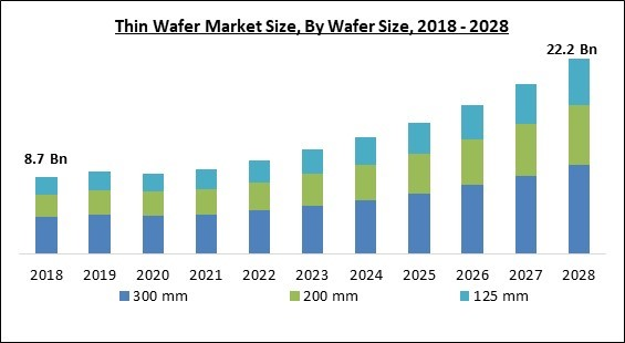
Based on the Wafer Size, the Thin Wafer Market is segmented into 125 mm, 200 mm, and 300 mm. The 300 mm segment acquired the highest revenue share in the thin wafer market in 2021. Due to their higher yield, 300 mm wafers are increasingly being used in applications like LED, which is boosting the thin wafer market's expansion. These wafers provide the scale economies and increased profitability that LED makers now find to be necessary. With the help of these wafers, producers may create a large number of products in a single batch.Technology Outlook
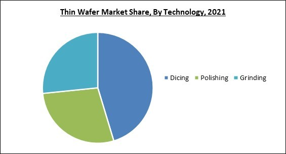
By Technology, the Thin Wafer Market is classified into Grinding, Polishing, and Dicing. The grinding segment recorded a substantial revenue share in the thin wafer market in 2021. To enable stacking and high-density packing of integrated circuits, the wafer thickness is decreased during the semiconductor device manufacture process known as wafer backgrounding (IC). On thin wafers that undergo several processing processes, ICs are created.Application Outlook
Based on the Application, the Thin Wafer Market is bifurcated into MEMS, CIS, Memory, RF Devices, LED, Interposer, Logic, and Others. The memory segment garnered the highest revenue share in the thin wafer market in 2021. Memory has relied mainly on a mixture of blades and laser dicing to separate complicated stacks. The high metal concentration causes delamination problems when just blade dicing is used on top layers. However, it is challenging to simulate 50 m thin wafers safely.Regional Outlook
Region-wise, the Thin Wafer Market is analyzed across North America, Europe, Asia Pacific, and LAMEA.The Asia Pacific segment acquired the highest revenue share in the thin wafer market in 2021. Due to China's and Japan's explosive growth in the use of high-end consumer goods, including smartwatches and smart home gadgets. Due to good economic conditions and rising consumer electronics demand, the Asia Pacific region is predicted to experience significant growth in the semiconductor market.The market research report covers the analysis of key stakeholders of the market. Key companies profiled in the report include Shin-Etsu Chemical Co., Ltd., SUMCO Corporation, GlobalWafers Co., Ltd., Siltronic AG, SK Siltron Co., Ltd., SUSS MicroTec SE, Soitec, DISCO Corporation, 3M Company, and Applied Materials, Inc.
Strategies Deployed in Thin Wafer Market
- May-2022: Soitec launched a 200 mm silicon carbide SmartSiC wafer. With this launch, Soitec would broaden its SiC product offering a further 150 mm, take the production of its SmartSiC wafers to the next grade, and meet the increasing demand of the automotive industry.
- Mar-2022: Wafer supplier Soitec expanded its geographical footprint by establishing a fabrication facility at its headquarters in Bernin, France. This expansion would fulfill the need for silicon carbide for electric vehicles and industrial purposes, with wafers produced utilizing the SmartSiC production procedure. Moreover, it would sustain the production of 300mm diameter silicon-on-insulator (SOI) wafers.
- Nov-2021: Soitec completed the acquisition of NOVASiC, an advanced technology business specializing in polishing and reclaiming wafers on silicon carbide. With this acquisition, Soitec would propel the growth of semiconductors for power supply systems in industrial and electromobility applications.
- Sep-2019: SK Siltron completed the acquisition of DuPont's wafer business, which manufactures a broad array of industrial chemicals, and synthetic fibers. With this acquisition, DuPont's SiC unit would provide SK Siltron with a sturdy wafer supply and develop synergy within the group.
- May-2019: Soitec took over EpiGaN, a foremost European supplier of GaN epitaxial wafer (epi-wafer) materials. Under this acquisition, EpiGaN would develop new supplementary growth possibilities within Soitec’s living Power-SOI products given GaN’s benefit in power transistor structures.
- Mar-2019: Soitec joined hands with Agency for Science, Technology and Research's (A*STAR) Institute of Microelectronics. Together, the companies aimed to design and incorporate a new layer transfer process within developed wafer-level multi-chip packaging techniques. Additionally, IME's Fan-Out Wafer Level Packaging (FOWLP) and 2.5D Through Silicon Interposer (TSI) technologies along with Soitec's Smart Cut(TM) technology, the latest cost-competitive approach delivers energy efficiency, higher commission, and improved product output.
- Feb-2019: SUSS MicroOptics expanded its geographical footprint by establishing an excellence center in Neuchâtel Switzerland for manufacturing wafer-level optics. This expansion aimed to satisfy the need for precision optics applications.
- Dec-2018: DISCO Corporation introduced DFG8640, a new completely automatic grinder consistent with 8-inch wafers and capable to grind a broad variety of materials, such as silicon, LiNbO3, LiTaO3, and SiC. The new DFG8640 contains high accuracy grinding; optimizing the processing point layout decreases consistency variation for both separate wafers and between wafers; a new spindle with high stability, lower vibration, and minor rotation speed change.
Scope of the Study
By Wafer Size
- 300 mm
- 200 mm
- 125 mm
By Technology
- Dicing
- Polishing
- Grinding
By Application
- Memory
- LED
- MEMS
- CIS
- RF Devices
- Interposer
- Logic
- Others
By Geography
- North America
- US
- Canada
- Mexico
- Rest of North America
- Europe
- Germany
- UK
- France
- Russia
- Spain
- Italy
- Rest of Europe
- Asia Pacific
- China
- Japan
- India
- South Korea
- Singapore
- Malaysia
- Rest of Asia Pacific
- LAMEA
- Brazil
- Argentina
- UAE
- Saudi Arabia
- South Africa
- Nigeria
- Rest of LAMEA
Key Market Players
List of Companies Profiled in the Report:
- Shin-Etsu Chemical Co., Ltd.
- SUMCO Corporation
- GlobalWafers Co., Ltd.
- Siltronic AG
- SK Siltron Co., Ltd.
- SUSS MicroTec SE
- Soitec
- DISCO Corporation
- 3M Company
- Applied Materials, Inc.
Unique Offerings
- Exhaustive coverage
- The highest number of market tables and figures
- Subscription-based model available
- Guaranteed best price
- Assured post sales research support with 10% customization free
Table of Contents
Companies Mentioned
- Shin-Etsu Chemical Co., Ltd.
- SUMCO Corporation
- GlobalWafers Co., Ltd.
- Siltronic AG
- SK Siltron Co., Ltd.
- SUSS MicroTec SE
- Soitec
- DISCO Corporation
- 3M Company
- Applied Materials, Inc.
Table Information
| Report Attribute | Details |
|---|---|
| No. of Pages | 228 |
| Published | October 2022 |
| Forecast Period | 2021 - 2028 |
| Estimated Market Value ( USD | $ 9602 Million |
| Forecasted Market Value ( USD | $ 22218 Million |
| Compound Annual Growth Rate | 13.0% |
| Regions Covered | Global |
| No. of Companies Mentioned | 10 |


