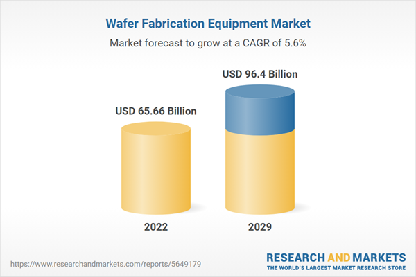
Wafer Fabrication Equipment Market is projected to grow at a CAGR of 5.64% during the forecast period to reach US$96.395 billion by 2029, from US$65.664 billion in 2022.
A wafer is a piece of silicon or other semiconductor material, designed in the form of a very thin disc. Wafer fabrication is a process that has been developed using various types of affirmative methods to develop photonic or several types of fully electrical circuits on the given or respective semiconductor wafers. Wafer fabrication is directly used to build and develop components with the given electrical structures.Market Drivers:
Growing demand from the consumer electronics industry
Semiconductor wafer fabrication finds diverse applications in the consumer electronics sector, spanning audio/video devices and various forms of entertainment products, including televisions, smartphones, pagers, copiers, and automotive components. The typical process involves multiple chemical steps to create semiconductor devices.The escalating demand for consumer electronics and devices is significantly driving the expansion of the fabrication equipment market. In 2022, U.S. imports of cellular phones reached 178 million units. Additionally, the market is experiencing growth due to increased investments in research and development as well as a focus on product innovation.
Innovation in semiconductor technology
Artificial Intelligence (AI) has been rolled out across industry verticals like research, healthcare, high-tech, and consumer electronics. To support AI-integrated circuits, improvements in semiconductor architectures have been urged to speed the movement of data in and out of memory with increased power and more efficient memory systems.Apart from AI, other innovations in the form of gravitational wave detectors, battery-free sensors for the medical industry, mobile CMOS imagers, MEMS Vibrational Energy Harvesters for IoT, etc., rely on semiconductor technologies extensively. These novel innovations are factoring into the market for wafer fabrication equipment.
Market Restraint:
Huge investments
Although the fabrication equipment market is witnessing growth, factors such as the requirement of very specific raw materials, state-of-the-art machinery requirements, and huge investments bring challenges to emerging market players, thus restricting the growth of the market.The global wafer fabrication equipment market is segmented by equipment type into oxidation systems, diffusion systems, epitaxial reactors, photolithography equipment, and others.
The global wafer fabrication equipment market is categorized by equipment type, including oxidation systems, diffusion systems, epitaxial reactors, photolithography equipment, and other miscellaneous equipment. Oxidation systems play a crucial role in generating a thin oxide layer on the silicon wafer surface, achieved through high temperatures and the introduction of oxygen or steam. Diffusion systems are responsible for incorporating dopant atoms into the silicon wafer, thereby modifying its electrical conductivity.
Epitaxial reactors facilitate the deposition of a single-crystal silicon layer on the wafer surface, enabling the creation of transistors. Photolithography equipment is instrumental in shaping the desired circuit layout onto the wafer using light and a photosensitive resist material. The "Others" category encompasses a diverse array of equipment utilized in various wafer fabrication processes.
APAC is anticipated to hold a significant share of the wafer fabrication equipment market.
By geography, the Asia-Pacific region is poised to show the fastest growth rate in the market. This is attributed to the development of foundries in China, Japan, and Taiwan and the increasing demand for consumer electronics.Market Developments:
- July 2023- Analog Devices, Inc., a prominent global semiconductor leader, celebrated its investment of over $1 billion to expand its semiconductor wafer fab in Beaverton, Oregon. The facility investment expanded cleanroom space to approximately 118,000 sq-ft and nearly doubled internal manufacturing capacity for products operating on the 180-nanometer technology node and above.
- June 2023- Lam Research Corp. introduced Coronus DX, hailed as the world's first bevel deposition solution, aimed at enhancing yield in chip production. This innovative solution was optimized to tackle crucial manufacturing challenges in next-generation logic, 3D NAND, and advanced packaging applications.
- November 2022- Lam Research Corp. announced the successful completion of the acquisition of SEMSYSCO GmbH, a worldwide supplier of wet processing semiconductor equipment, from Gruenwald Equity and other investors. Through the integration of SEMSYSCO, Lam enhanced its capabilities in advanced packaging, particularly for cutting-edge logic chips and chipset-based solutions catering to high-performance computing (HPC), artificial intelligence (AI), and other data-intensive applications.
Market Segmentation:
By Equipment Type
- Oxidation Systems
- Diffusion Systems
- Epitaxial Reactors
- Photolithography Equipment
- Others
By Size
- 50 mm-100 mm
- 100 mm-200 mm
- 200 mm-300 mm
- 300 mm-450 mm
By Geography
- Americas
- USA
- Others
- Europe Middle East and Africa
- Germany
- France
- Israel
- Others
- Asia Pacific
- China
- Japan
- South Korea
- Taiwan
- Others
Table of Contents
Companies Mentioned
- LAM RESEARCH CORPORATION
- SCREEN Semiconductor Solutions Co., Ltd
- Tokyo Electron Limited
- Pacifica Partners Inc
- Hitachi High-Technologies Corporation
- KLA-Tencor Corporation
Table Information
| Report Attribute | Details |
|---|---|
| No. of Pages | 121 |
| Published | March 2024 |
| Forecast Period | 2022 - 2029 |
| Estimated Market Value ( USD | $ 65.66 Billion |
| Forecasted Market Value ( USD | $ 96.4 Billion |
| Compound Annual Growth Rate | 5.6% |
| Regions Covered | Global |
| No. of Companies Mentioned | 6 |


