Speak directly to the analyst to clarify any post sales queries you may have.
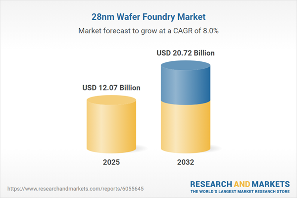
The 28nm Wafer Foundry Market grew from USD 11.21 billion in 2024 to USD 12.06 billion in 2025. It is expected to continue growing at a CAGR of 7.75%, reaching USD 17.56 billion by 2030.
Unveiling the Fundamentals and Strategic Significance of the 28nm Wafer Foundry Landscape and Market Dynamics in Today’s Semiconductor Ecosystem
In the rapidly evolving landscape of semiconductor manufacturing, the 28nm wafer foundry segment occupies a pivotal role. As the industry navigates between the push for advanced nodes and the sustained demand for mature processes, the 28nm node delivers a strategic balance of performance, power efficiency, and cost-effectiveness. Its versatility underpins a wide array of applications ranging from automotive safety systems to high-bandwidth networking equipment.
As market dynamics shift under the influence of supply chain optimization, geopolitical tensions, and technological convergence, foundry operators at the 28nm node have encountered both challenges and opportunities. Capacity constraints, material availability, and regulatory frameworks intersect with rising demand for connectivity and computing power, prompting a recalibration of investment priorities and operational models. Stakeholders are compelled to align process innovation with agile manufacturing practices to maintain competitiveness.
This executive summary distills the core themes shaping the 28nm wafer foundry landscape. It provides an overview of transformative technological developments, regulatory impacts, segmentation insights, and regional dynamics. By synthesizing primary research inputs and expert interviews, this summary equips decision-makers with a cohesive understanding of current imperatives and actionable pathways to fortify strategic positioning within the 28nm domain.
As such, this document is tailored for senior executives, operations leaders, and strategic planners seeking to deepen their comprehension of the 28nm segment’s trajectory. It highlights critical signals, underexplored niches, and collaborative strategies that can unlock value across the foundry ecosystem. Through this lens, organizations can anticipate emerging inflection points and align resource deployment with sustainable growth objectives.
Examining the Disruptive Technological Innovations and Industry Realignments That Are Redefining Competitive Forces within the 28nm Wafer Fabrication Sector
Advancements in lithography and materials science have catalyzed a wave of process enhancements at the 28nm node, transcending traditional CMOS paradigms. The introduction of more precise etching techniques and novel dielectric films has elevated device performance while containing leakage currents. Simultaneously, the integration of advanced packaging solutions such as wafer-level chip-scale packages has redefined thermal management and form factor constraints, enabling higher device densities and improved signal integrity.
Operational frameworks within foundries have also undergone significant realignment. The integration of real-time analytics and machine learning-driven yield optimization tools has sharpened production efficiency, reducing cycle times and defect rates. Moreover, the industry’s pivot towards more sustainable manufacturing practices-embracing water recycling, energy recovery, and lower global warming potential chemicals-reflects broader ESG imperatives. These shifts have been accompanied by strategic consolidation among equipment suppliers and strategic partnerships between process licensors and capacity providers.
Collectively, these developments have recalibrated competitive dynamics, shifting the basis of differentiation from mere capacity expansion to a more holistic value proposition that interweaves technological excellence with environmental stewardship and supply chain resilience. Industry players that embrace this multifaceted transformation can secure a durable competitive edge in the increasingly complex 28nm wafer fabrication landscape.
Assessing the Multidimensional Effects of United States Tariff Adjustments Scheduled for 2025 on the 28nm Wafer Foundry Supply Chain and Trade Flows
The imposition of revised tariff schedules by the United States effective in 2025 has introduced a new layer of complexity into the global wafer foundry supply chain. Incremental duties on critical raw materials and key equipment components have amplified procurement costs, compelling foundry operators to reassess long-lead sourcing strategies. In response, many suppliers have accelerated localization efforts, establishing alternate supply nodes in tariff-exempt jurisdictions to mitigate cost exposure.
These trade policy adjustments have also prompted companies to rethink inventory management and contractual frameworks. Longer forecast horizons and buffer stock allocations have become more prevalent as stakeholders aim to preempt price fluctuations. At the same time, equipment vendors are exploring modular manufacturing platforms that can be configured regionally, thereby reducing cross-border transport obligations and attendant duties. Such initiatives underscore the growing importance of agile manufacturing networks.
As a result, the costs associated with wafer fabrication are now influenced as much by geopolitical considerations as by process complexity. Companies that proactively adapt to the evolving tariff environment-through diversification of supplier portfolios, renegotiated terms with original equipment manufacturers, and strategic shifts toward domestic or friendly foreign capacity-are better positioned to absorb cost pressures without compromising on technology roadmaps or time-to-market objectives.
Deciphering Core Market Dimensions through Technology, Production Capacity, and End-Use Application Perspectives in the 28nm Wafer Foundry Domain
Analysis of the 28nm wafer foundry market through multiple strategic lenses reveals distinct performance drivers and segmentation patterns. When viewed by technology, the industry’s offerings encompass the established 28nm PolySiON process, a workhorse solution for mainstream logic and mixed-signal devices; the bulk CMOS variant, which remains a dependable choice for high-volume memory and power management applications; and the emerging fully depleted silicon-on-insulator technology, prized for its low leakage and high-frequency characteristics, particularly in RF and niche IoT components.
Considering production capacity, large-scale facilities have leveraged economies of scale to deliver competitive unit costs and rapid cycle throughput, making them ideal for high-volume consumer electronics and networking infrastructure. Mid-scale operations, by contrast, emphasize flexibility, tailoring production batches to meet specialized requirements in automotive safety modules and industrial automation controls. In smaller-scale environments, foundries often concentrate on bespoke runs and prototype services, supporting emerging startups and differentiated product horizons where agility outweighs sheer output.
The breakdown by end-use application further underscores the diverse value propositions inherent to the 28nm process node. The automotive electronics sector, encompassing advanced driver-assistance systems, electric vehicle power modules, and sophisticated infotainment units, demands stringent reliability and temperature resilience. Within consumer electronics, the smartphone, tablet, and wearable markets drive relentless cycles of miniaturization and power efficiency. Industrial consumers, from IoT device integrators to robotics innovators and sensor manufacturers, require robust performance under variable operating conditions. Networking and communication deployments, including 5G base stations, optical network devices, and routers and switches, depend on high-speed signaling and low-latency interfaces, all achievable within the 28nm parameter set.
Revealing Strategic Regional Dynamics Driving Growth Patterns and Investment Priorities across Americas Europe Middle East Africa and Asia-Pacific Wafer Foundry
A regional perspective on the 28nm wafer foundry market highlights divergent growth trajectories and strategic imperatives across major geographies. In the Americas, capacity expansions are driven by a confluence of governmental incentives and reshoring initiatives. Lower transportation costs to key automotive and aerospace customers combine with supportive regulatory frameworks to spur investment in both green-field fab construction and retrofitting of existing facilities. Collaboration between ecosystem stakeholders has also accelerated, with a notable uptick in joint ventures and technology licensing agreements.
Europe, the Middle East, and Africa showcase a mosaic of policy-driven demand signals and nascent capacity development. While European Union directives on sustainability and digital sovereignty push for localized semiconductor production, some regions in the Middle East are leveraging sovereign wealth to underwrite large-scale fabrication projects. In contrast, African markets are gradually maturing, with early-stage partnerships focusing on skills development and small-scale assembly, laying a foundation for future vertical integration.
In the Asia-Pacific arena, the 28nm node remains at the heart of a sprawling manufacturing ecosystem. Established foundries continue to refine process yields and diversify end-market applications, while emerging players in Southeast Asia explore specialized capacity niches. Robust domestic demand in consumer electronics, burgeoning automotive semiconductor content, and government-backed R&D consortia reinforce the region’s position as the epicenter of 28nm wafer foundry activity. Taken together, these regional dynamics underscore the need for a geographically balanced strategy that leverages local strengths while mitigating exposure to policy shifts.
Illuminating Leading Foundry Players and Partnership Trends Shaping Technological Progress and Capacity Enhancement within the Global 28nm Fabrication Ecosystem
Leading foundry operators have charted varied strategic paths to secure leadership at the 28nm process node. Taiwan Semiconductor Manufacturing Company has sustained its edge through incremental process refinements and capacity expansion in both Mainland Asia and North America, positioning itself as a preferred partner for global IDMs and fabless designers. Samsung Foundry has mirrored this trajectory with dual-track investments in advanced packaging and differentiated FD-SOI offerings, widening its addressable market.
GlobalFoundries has focused on operational excellence and client-centric service models, leveraging modular fab designs and rapid process qualification cycles to cater to both high-volume consumer electronics brands and aerospace-qualified suppliers. United Microelectronics Corporation has pursued a hybrid strategy, combining stable bulk CMOS production with targeted roll-out of polysilicon-based enhancements, thus balancing cost pressures with performance gains. China-based foundries such as SMIC have scaled production capacity aggressively, driven by domestic demand and strategic collaborations aimed at technology transfer and ecosystem development.
Across this landscape, partnership strategies have emerged as a critical determinant of success. Foundry operators are forging alliances with equipment vendors to co-innovate on next-generation chemical formulations and lithography solutions. At the same time, cross-industry consortia are aligning process roadmaps with emerging standards in automotive and networking sectors, thereby accelerating time-to-market and ensuring robust compliance across rigorous qualification regimes. Companies that deftly blend internal R&D with external collaboration stand to consolidate their market positioning in the fiercely competitive 28nm domain.
Formulating Targeted Strategic Imperatives and Operational Enhancements to Propel Competitive Positioning and Long-Term Resilience in the 28nm Foundry Sector
Industry leaders seeking to fortify their presence in the 28nm wafer foundry space should adopt a multidimensional approach that addresses both technological and operational vectors. Investing in advanced metrology and inline inspection systems will not only improve yield optimization but also reduce cycle times and enhance defect detection at critical process junctures. Parallel to this, expanding cloud-based analytics infrastructure can enable predictive maintenance and real-time quality monitoring, fostering proactive decision-making and minimizing unplanned downtime.
Capacity diversification is another pivotal lever; by deploying additional lines in tariff-friendly regions and leveraging strategic partnerships to share capital expenditures, companies can mitigate geopolitical risks and optimize overall asset utilization. Embracing green manufacturing practices-such as closed-loop water systems and the utilization of low global-warming-potential process chemicals-will align operations with emerging environmental mandates and drive long-term cost efficiencies. Equally important is the cultivation of talent through targeted training programs and cross-industry talent exchanges, ensuring that specialized skills in lithography and process integration remain robust.
Finally, collaboration with key ecosystem partners, including material suppliers and equipment original equipment manufacturers, can accelerate the development of next-generation process enhancements. By integrating these recommendations into their strategic playbooks, industry incumbents and new entrants alike can leverage the 28nm node as a launchpad for innovation, resilience, and sustained growth.
Outlining Rigorous Primary and Secondary Research Processes Employed to Derive Insightful Data and Analytical Validity for the 28nm Foundry Study
The research methodology underpinning this report integrates both primary and secondary research protocols to ensure comprehensive coverage and analytical rigor. Primary research was conducted through in-depth interviews with senior executives, process engineers, and supply chain leaders across leading foundry organizations and their key suppliers. Supplementary surveys and workshops facilitated interactive validation of emerging themes and triangulated viewpoints on process adoption, capacity investments, and policy impacts.
Secondary research encompassed an exhaustive review of industry publications, patent filings, regulatory announcements, and technical whitepapers. Data from trade associations, governmental agencies, and market intelligence databases provided contextual backing for macroeconomic and geopolitical analyses. A systematic data triangulation approach was applied to reconcile discrepancies between multiple information sources, ensuring consistency and credibility in the insights derived.
Quality assurance mechanisms included cross-referencing quantitative findings with qualitative expert opinions and conducting internal peer reviews by semiconductor domain specialists. All analytical models were stress-tested under various scenario parameters to confirm robustness and sensitivity. This blended research framework ensures that the conclusions and recommendations presented are grounded in both empirical evidence and strategic foresight.
Synthesizing Key Learnings and Forward-Looking Perspectives to Guide Strategic Decisions and Innovation Pathways in the 28nm Foundry Arena
This executive summary has synthesized the critical themes shaping the 28nm wafer foundry sector, from technological breakthroughs to geopolitical realignments and nuanced segmentation dynamics. The convergence of advanced process innovations, such as enhanced dielectric materials and next-generation packaging, with evolving trade policies underscores the importance of an integrated strategic framework. Stakeholders must navigate these converging forces to maintain operational excellence and market relevance.
By applying a multidimensional lens-examining technology variants, capacity modalities, and end-use demand profiles-organizations can pinpoint high-value opportunities and tailor service offerings accordingly. Regional considerations further inform strategic deployment of resources, leveraging incentives and mitigating exposure to policy volatility. The review of leading foundry players demonstrates that a balanced investment in internal R&D, ecosystem partnerships, and flexible capacity planning is paramount.
Looking ahead, the industry’s ability to adapt to tariff adjustments, supply chain reconfiguration, and sustainability imperatives will largely determine the competitive hierarchy within the 28nm domain. Continuous monitoring of policy trajectories, coupled with agile process development and talent cultivation, will be vital. The insights and recommendations outlined herein serve as a strategic compass, guiding decision-makers in charting a resilient and innovation-driven path forward.
Market Segmentation & Coverage
This research report categorizes to forecast the revenues and analyze trends in each of the following sub-segmentations:
- Technology
- 28nm PolySiON
- Bulk CMOS
- Fully Depleted Silicon-On-Insulator
- Production Capacity
- Large-Scale Production
- Mid-Scale Production
- Small-Scale Production
- End-Use
- Automotive Electronics
- Advanced Driver-Assistance Systems
- Electric Vehicles
- Infotainment Systems
- Computing
- Consumer Electronics
- Smartphones
- Tablets
- Wearables
- Industrial
- IoT Devices
- Robotics
- Sensors
- Networking & Communication
- 5G Base Stations
- Optical Network Devices
- Routers & Switches
- Automotive Electronics
This research report categorizes to forecast the revenues and analyze trends in each of the following sub-regions:
- Americas
- United States
- California
- Texas
- New York
- Florida
- Illinois
- Pennsylvania
- Ohio
- Canada
- Mexico
- Brazil
- Argentina
- United States
- Europe, Middle East & Africa
- United Kingdom
- Germany
- France
- Russia
- Italy
- Spain
- United Arab Emirates
- Saudi Arabia
- South Africa
- Denmark
- Netherlands
- Qatar
- Finland
- Sweden
- Nigeria
- Egypt
- Turkey
- Israel
- Norway
- Poland
- Switzerland
- Asia-Pacific
- China
- India
- Japan
- Australia
- South Korea
- Indonesia
- Thailand
- Philippines
- Malaysia
- Singapore
- Vietnam
- Taiwan
This research report delves into recent significant developments and analyzes trends in each of the following companies:
- GlobalFoundries Inc.
- Infineon Technologies AG
- Intel Corporation
- Micron Technology Inc.
- Powerchip Technology Corporation
- Qualcomm Technologies, Inc.
- Renesas Electronics Corporation
- ROHM Co., Ltd.
- Samsung Electronics Co., Ltd.
- Semiconductor Manufacturing International Corporation (SMIC)
- Shanghai Huali Microelectronics Corp (HLMC) by Huahong Group
- STMicroelectronics NV
- Taiwan Semiconductor Manufacturing Company (TSMC)
- Texas Instruments Incorporated
- United Microelectronics Corporation (UMC)
Table of Contents
Samples
LOADING...
Companies Mentioned
The companies profiled in this 28nm Wafer Foundry market report include:- GlobalFoundries Inc.
- Infineon Technologies AG
- Intel Corporation
- Micron Technology Inc.
- Powerchip Technology Corporation
- Qualcomm Technologies, Inc.
- Renesas Electronics Corporation
- ROHM Co., Ltd.
- Samsung Electronics Co., Ltd.
- Semiconductor Manufacturing International Corporation (SMIC)
- Shanghai Huali Microelectronics Corp (HLMC) by Huahong Group
- STMicroelectronics NV
- Taiwan Semiconductor Manufacturing Company (TSMC)
- Texas Instruments Incorporated
- United Microelectronics Corporation (UMC)
Table Information
Report Attribute | Details |
---|---|
No. of Pages | 199 |
Published | August 2025 |
Forecast Period | 2025 - 2030 |
Estimated Market Value ( USD | $ 12.06 billion |
Forecasted Market Value ( USD | $ 17.56 billion |
Compound Annual Growth Rate | 7.7% |
Regions Covered | Global |
No. of Companies Mentioned | 16 |