Global Epitaxial Wafer and Chip Technology Market - Key Trends & Drivers Summarized
Why Is Epitaxial Wafer and Chip Technology Fundamental to the Next Generation of Semiconductor Devices?
Epitaxial wafer and chip technology plays a pivotal role in the advancement of modern semiconductor devices, enabling the development of high-performance, energy-efficient, and reliable integrated circuits used in a wide range of electronic applications. Epitaxy, the process of growing a crystalline layer on a substrate wafer with atomic-level precision, provides a defect-free foundation essential for the fabrication of advanced microelectronic and optoelectronic devices. This technique allows for superior control over material properties such as doping concentration, thickness, and uniformity, which are critical in tailoring electronic behavior for specific device applications. Epitaxial wafers are widely used in power electronics, RF components, LEDs, laser diodes, and CMOS logic devices, particularly in sectors like telecommunications, automotive, consumer electronics, and aerospace. As the demand for faster, smaller, and more efficient chips increases, the use of epitaxial layers enables designers to push the boundaries of Moore's Law, particularly in high-voltage and high-frequency applications. Furthermore, the rise of compound semiconductors such as gallium nitride (GaN) and silicon carbide (SiC) in power electronics heavily relies on epitaxial growth techniques to enhance switching performance and thermal stability. With the global race for semiconductor dominance intensifying, epitaxial wafer and chip technology is now seen not just as a production tool, but as a strategic asset underpinning national security, industrial growth, and digital transformation.How Are Technological Advancements Expanding the Capabilities of Epitaxial Wafer and Chip Production?
Technological innovation is significantly enhancing the capabilities of epitaxial wafer and chip production, driving improvements in efficiency, scalability, and material diversity. Advances in chemical vapor deposition (CVD), molecular beam epitaxy (MBE), and metal-organic chemical vapor deposition (MOCVD) are enabling ultra-thin, high-purity epitaxial layers with atomic-level control over material composition and doping profiles. These methods are now being adapted to new substrate materials beyond traditional silicon - including SiC, GaN, gallium arsenide (GaAs), and indium phosphide (InP) - to meet the specialized requirements of high-power, high-frequency, and optoelectronic devices. Automation and precision metrology systems integrated into epitaxy tools are enhancing yield rates by reducing variability and detecting defects in real time. Additionally, advanced thermal management and wafer handling techniques are allowing manufacturers to scale up production to 200mm and 300mm wafer sizes, reducing cost per die and improving throughput. Hybrid epitaxy methods, such as selective area growth and epitaxial lateral overgrowth, are also being developed to enable three-dimensional integration and heterogeneous chip stacking - paving the way for more compact and multifunctional chip architectures. Furthermore, the application of AI-driven process control and digital twins is helping fabs predict growth behavior, optimize recipes, and reduce development time. These advances are positioning epitaxial wafer and chip technology at the forefront of semiconductor innovation, enabling the industry to address emerging challenges in quantum computing, 6G communications, and automotive electrification.Why Is the Demand for Epitaxial Wafers and Chips Growing Across Multiple End-Use Markets?
The demand for epitaxial wafers and chips is accelerating globally as multiple high-growth sectors increasingly rely on precision-engineered semiconductor materials for next-generation device performance. In the power electronics industry, SiC-based epitaxial wafers are enabling compact, energy-efficient inverters and converters for electric vehicles (EVs), renewable energy systems, and smart grids - supporting the global transition toward sustainable energy. In telecommunications, GaN-based RF epitaxial wafers are essential for the development of high-frequency amplifiers and transceivers used in 5G base stations, satellite communication, and radar systems. The consumer electronics market continues to benefit from epi-enabled CMOS and optoelectronic chips, which power everything from smartphones and wearable devices to 4K displays and biometric sensors. Meanwhile, the automotive industry is integrating more epitaxial devices for advanced driver-assistance systems (ADAS), battery management systems, and vehicle-to-everything (V2X) communication modules. Medical technology is another fast-growing application area, where epi wafers are used in laser diodes and optical sensors for diagnostic equipment and surgical tools. Even in industrial automation and defense, epitaxial wafers support robust, high-power electronics required for harsh operating environments. These wide-ranging applications are expanding the addressable market for epi-based technologies, encouraging strategic investments in new fabs, wafer foundries, and materials R&D across North America, Asia-Pacific, and Europe. As device complexity and performance demands continue to rise, epitaxial technology is emerging as a foundational enabler across nearly every vertical of the modern digital economy.What Key Drivers Are Accelerating the Growth of the Epitaxial Wafer and Chip Technology Market?
The growth in the epitaxial wafer and chip technology market is being driven by a confluence of factors spanning technological evolution, geopolitical strategy, market demand, and sustainability imperatives. One of the primary drivers is the escalating need for high-performance semiconductors in fast-growing domains such as EVs, data centers, 5G/6G infrastructure, and AI accelerators - each of which demands precise control over material properties and device performance that only epitaxy can deliver. The global semiconductor supply chain reorganization, spurred by chip shortages and geopolitical tensions, is prompting countries to localize advanced semiconductor manufacturing, which includes the expansion of epitaxy production capacity. Government initiatives like the U.S. CHIPS Act, the EU Chips Act, and China's “Made in China 2025” plan are funding the development of domestic epitaxial capabilities to secure technological independence and economic resilience. Environmental regulations are also playing a role, as energy-efficient power devices built on epitaxial wafers help reduce global carbon emissions and meet climate targets. Additionally, increasing R&D investments by semiconductor giants and specialty material providers are accelerating breakthroughs in wafer scalability, material quality, and integration technologies. Mergers, partnerships, and acquisitions across the semiconductor ecosystem are streamlining innovation pipelines and facilitating faster commercialization of epitaxial technologies. Finally, growing interest in emerging fields such as quantum computing, silicon photonics, and neuromorphic chips is generating new demand for custom-engineered epitaxial substrates with ultra-low defect densities and exotic material combinations. These multifaceted growth drivers are setting the stage for a strong and sustained expansion of the global epitaxial wafer and chip technology market.Report Scope
The report analyzes the Epitaxial Wafer and Chip Technology market, presented in terms of market value (US$). The analysis covers the key segments and geographic regions outlined below:- Segments: Material (Gallium, Arsenic, Gallium Nitride, Gallium Arsenide, Indium Phosphide Gallium Arsenide, Indium Phosphide, Other Materials); Application (Microelectronics, Optoelectronics, RF Microwave Applications, Other Applications); Wafer Size (50 - 100 mm, 100 -150 mm, 150 - 200 mm, Above 200mm).
- Geographic Regions/Countries: World; United States; Canada; Japan; China; Europe (France; Germany; Italy; United Kingdom; Spain; Russia; and Rest of Europe); Asia-Pacific (Australia; India; South Korea; and Rest of Asia-Pacific); Latin America (Argentina; Brazil; Mexico; and Rest of Latin America); Middle East (Iran; Israel; Saudi Arabia; United Arab Emirates; and Rest of Middle East); and Africa.
Key Insights:
- Market Growth: Understand the significant growth trajectory of the Gallium Material segment, which is expected to reach US$386.5 Million by 2030 with a CAGR of a 68.9%. The Arsenic Material segment is also set to grow at 50.9% CAGR over the analysis period.
- Regional Analysis: Gain insights into the U.S. market, valued at $17.8 Million in 2024, and China, forecasted to grow at an impressive 72% CAGR to reach $283.9 Million by 2030. Discover growth trends in other key regions, including Japan, Canada, Germany, and the Asia-Pacific.
Why You Should Buy This Report:
- Detailed Market Analysis: Access a thorough analysis of the Global Epitaxial Wafer and Chip Technology Market, covering all major geographic regions and market segments.
- Competitive Insights: Get an overview of the competitive landscape, including the market presence of major players across different geographies.
- Future Trends and Drivers: Understand the key trends and drivers shaping the future of the Global Epitaxial Wafer and Chip Technology Market.
- Actionable Insights: Benefit from actionable insights that can help you identify new revenue opportunities and make strategic business decisions.
Key Questions Answered:
- How is the Global Epitaxial Wafer and Chip Technology Market expected to evolve by 2030?
- What are the main drivers and restraints affecting the market?
- Which market segments will grow the most over the forecast period?
- How will market shares for different regions and segments change by 2030?
- Who are the leading players in the market, and what are their prospects?
Report Features:
- Comprehensive Market Data: Independent analysis of annual sales and market forecasts in US$ Million from 2024 to 2030.
- In-Depth Regional Analysis: Detailed insights into key markets, including the U.S., China, Japan, Canada, Europe, Asia-Pacific, Latin America, Middle East, and Africa.
- Company Profiles: Coverage of players such as Abbott, Ad-Tech Medical Instrument Corporation, Auris Health Inc. (Hansen Medical), Boston Scientific, Cephalon Inc. (Teva Pharmaceuticals) and more.
- Complimentary Updates: Receive free report updates for one year to keep you informed of the latest market developments.
Some of the 39 companies featured in this Epitaxial Wafer and Chip Technology market report include:
- AIXTRON SE
- Applied Materials, Inc.
- ASM International N.V.
- Coherent Corp (II-VI Incorporated)
- EpiGaN AS
- GlobalWafers Co., Ltd.
- IQE PLC
- KLA Corporation
- Mattson Technology, Inc.
- NuFlare Technology Inc.
- RIBER S.A.
- Siltronic AG
- SK Siltron Co., Ltd.
- Soitec
- SPTS Technologies (a KLA company)
- Sumco Corporation
- Sumitomo Electric Industries, Ltd.
- Tokyo Electron Limited
- Veeco Instruments Inc.
- WaferWorks Corporation
This edition integrates the latest global trade and economic shifts into comprehensive market analysis. Key updates include:
- Tariff and Trade Impact: Insights into global tariff negotiations across 180+ countries, with analysis of supply chain turbulence, sourcing disruptions, and geographic realignment. Special focus on 2025 as a pivotal year for trade tensions, including updated perspectives on the Trump-era tariffs.
- Adjusted Forecasts and Analytics: Revised global and regional market forecasts through 2030, incorporating tariff effects, economic uncertainty, and structural changes in globalization. Includes historical analysis from 2015 to 2023.
- Strategic Market Dynamics: Evaluation of revised market prospects, regional outlooks, and key economic indicators such as population and urbanization trends.
- Innovation & Technology Trends: Latest developments in product and process innovation, emerging technologies, and key industry drivers shaping the competitive landscape.
- Competitive Intelligence: Updated global market share estimates for 2025, competitive positioning of major players (Strong/Active/Niche/Trivial), and refined focus on leading global brands and core players.
- Expert Insight & Commentary: Strategic analysis from economists, trade experts, and domain specialists to contextualize market shifts and identify emerging opportunities.
Table of Contents
Companies Mentioned (Partial List)
A selection of companies mentioned in this report includes, but is not limited to:
- AIXTRON SE
- Applied Materials, Inc.
- ASM International N.V.
- Coherent Corp (II-VI Incorporated)
- EpiGaN AS
- GlobalWafers Co., Ltd.
- IQE PLC
- KLA Corporation
- Mattson Technology, Inc.
- NuFlare Technology Inc.
- RIBER S.A.
- Siltronic AG
- SK Siltron Co., Ltd.
- Soitec
- SPTS Technologies (a KLA company)
- Sumco Corporation
- Sumitomo Electric Industries, Ltd.
- Tokyo Electron Limited
- Veeco Instruments Inc.
- WaferWorks Corporation
Table Information
| Report Attribute | Details |
|---|---|
| No. of Pages | 390 |
| Published | January 2026 |
| Forecast Period | 2024 - 2030 |
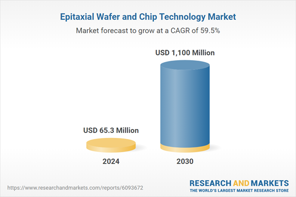
| Estimated Market Value ( USD | $ 65.3 Million |
| Forecasted Market Value ( USD | $ 1100 Million |
| Compound Annual Growth Rate | 59.5% |
| Regions Covered | Global |


