Global Photomask Repair Systems Market - Key Trends & Drivers Summarized
The photomask repair systems market is experiencing significant growth, driven by advancements in semiconductor manufacturing, increasing demand for smaller and more complex integrated circuits (ICs), and the shift toward extreme ultraviolet (EUV) lithography. As semiconductor fabrication nodes continue to shrink, with sub-7nm and 5nm process technologies becoming mainstream, the need for high-precision photomask repair solutions is more critical than ever. Photomasks, which are essential in the lithographic process of semiconductor manufacturing, serve as the blueprint for microchip production. Even the smallest defect on a photomask can lead to costly production errors, yield loss, and defective chips, necessitating precise, efficient, and automated repair systems.A major trend driving the market is the increasing complexity of mask designs, particularly with the adoption of multi-patterning techniques, extreme ultraviolet (EUV) lithography, and advanced deep ultraviolet (DUV) processes. The growing use of optical proximity correction (OPC) and phase shift masks (PSM) to enhance lithographic resolution has made photomask defect repair more challenging. Traditional repair techniques such as focused ion beam (FIB) and electron beam (e-beam) repair are evolving to handle the nanoscale accuracy requirements of next-generation semiconductor devices. In response, manufacturers are investing in AI-driven automated defect detection, high-resolution atomic force microscopy (AFM) analysis, and non-contact repair methodologies to improve mask repair efficiency and throughput.
Another critical driver is the escalating costs of photomasks and the push for extending mask lifespan. The production of advanced EUV masks requires complex multilayer structures and absorber materials, making them significantly more expensive than traditional DUV masks. As a result, semiconductor manufacturers are increasingly relying on advanced repair systems to extend the usability of masks, reduce scrap rates, and optimize cost efficiency. With EUV photomask blanks costing upwards of $100,000 each, effective repair solutions are essential to avoid costly replacements and ensure defect-free semiconductor production.
How Are Technological Advancements Reshaping Photomask Repair Systems?
The evolution of photomask repair technologies is being driven by the need for higher precision, increased automation, and the ability to repair defects at the atomic level. Traditional repair methods such as laser ablation, ion beam milling, and gas-assisted etching are being replaced or supplemented by next-generation repair techniques that offer higher accuracy and minimal impact on the mask structure.One of the most notable advancements in this field is the adoption of multi-beam electron microscopy (MBEM) and atomic layer deposition (ALD)-based repair. These methods allow for precise defect removal and atomic-level material deposition, ensuring that the repaired photomasks maintain their optical integrity and structural durability. In particular, e-beam-based localized deposition systems are gaining popularity for correcting EUV mask defects, where conventional etching-based methods may cause excessive material loss.
Another significant innovation is the integration of artificial intelligence (AI) and machine learning (ML) in defect inspection and repair processes. AI-driven defect recognition algorithms enable real-time, high-speed defect classification, reducing manual intervention and improving repair accuracy. These systems can automatically identify systematic and random defects, apply adaptive repair techniques, and minimize human-induced variability in the repair process. As semiconductor nodes become more advanced, AI-assisted repair solutions will become increasingly indispensable for maintaining high production yields.
Additionally, the rise of non-contact repair solutions, such as UV-induced atomic manipulation and laser-assisted defect repair, is transforming the market. These methods eliminate the risk of mechanical or ion-induced damage, making them ideal for repairing high-precision photomasks used in EUV lithography. As semiconductor manufacturers push toward 2nm and below fabrication nodes, next-generation photomask repair systems will need to incorporate nanoscale precision tools, automated feedback loops, and real-time defect correction mechanisms to keep pace with industry demands.
What Role Do End-Use Applications Play in the Growth of Photomask Repair Systems?
The increasing demand for high-performance computing (HPC), artificial intelligence (AI) chips, 5G infrastructure, and consumer electronics is driving the need for high-resolution photomasks and defect-free lithography processes. Semiconductor manufacturers are under pressure to deliver smaller, faster, and more power-efficient chips, which requires advanced photomask production and repair systems.In the foundry and logic chip manufacturing sector, companies like TSMC, Intel, and Samsung are leading the charge in sub-5nm semiconductor production, necessitating highly precise photomask repair solutions. The shift toward gate-all-around (GAA) transistors, 3D stacking, and heterogeneous integration further increases the complexity of photomasks, making defect management and repair a critical part of the semiconductor supply chain.
The memory industry, including DRAM and NAND flash manufacturers, also heavily relies on photomask repair technology. With increasing bit density and scaling challenges in 3D NAND architecture, maintaining high-yield mask quality is essential to prevent pattern distortion and feature degradation during the fabrication process. As next-generation memory technologies such as MRAM and ReRAM emerge, the need for advanced mask repair solutions that can handle ultra-fine patterns and high-aspect-ratio structures will continue to rise.
Another growing area of application is the automotive semiconductor industry, where power electronics, advanced driver-assistance systems (ADAS), and AI-driven vehicle processors require highly reliable semiconductor chips. Automotive-grade chips must meet strict quality and longevity requirements, making defect-free photomasks and high-precision repair solutions essential for ensuring consistent production quality and defect minimization.
What Are the Key Factors Driving the Growth of the Photomask Repair Systems Market?
The growth in the photomask repair systems market is driven by several factors, including advancements in semiconductor manufacturing, increasing photomask complexity, rising demand for EUV lithography, and the need for cost-efficient defect management solutions. The transition to sub-5nm process nodes is pushing the boundaries of defect detection and repair technologies, necessitating higher precision repair tools, AI-assisted automation, and ultra-high-resolution imaging systems.The growing adoption of EUV lithography in semiconductor fabrication is a major catalyst for market expansion. EUV photomasks have intricate multilayer structures and exotic absorber materials, making them highly susceptible to defects during manufacturing and handling. As EUV production scales up, semiconductor manufacturers are investing in specialized repair systems capable of correcting EUV mask defects with atomic precision, ensuring consistent chip performance and yield stability.
Another key factor is the rising cost of photomasks and mask sets. With each EUV photomask costing over $100,000, manufacturers are prioritizing repair over replacement to optimize production costs. The increasing mask usage lifecycle and demand for on-site repair capabilities are fueling investments in automated, in-line photomask repair solutions that minimize downtime and enhance operational efficiency.
Furthermore, the integration of AI and machine learning in defect inspection and repair workflows is streamlining high-speed defect classification, adaptive repair strategies, and precision material deposition techniques. As semiconductor manufacturers strive for higher yield rates and defect-free production, the demand for intelligent photomask repair solutions will continue to grow.
As the semiconductor industry advances toward next-generation computing, AI, IoT, and quantum computing technologies, photomask repair systems will play a critical role in sustaining innovation, cost efficiency, and high-yield production in the global semiconductor supply chain.
Report Scope
The report analyzes the Photomask Repair Systems market, presented in terms of market value (US$). The analysis covers the key segments and geographic regions outlined below:- Segments: Type (Laser Technology, Focused Ion Beam (FIB) Technology, Nanomachining Technology).
- Geographic Regions/Countries: World; United States; Canada; Japan; China; Europe (France; Germany; Italy; United Kingdom; Spain; Russia; and Rest of Europe); Asia-Pacific (Australia; India; South Korea; and Rest of Asia-Pacific); Latin America (Argentina; Brazil; Mexico; and Rest of Latin America); Middle East (Iran; Israel; Saudi Arabia; United Arab Emirates; and Rest of Middle East); and Africa.
Key Insights:
- Market Growth: Understand the significant growth trajectory of the Laser Technology segment, which is expected to reach US$14 Billion by 2030 with a CAGR of a 9.1%. The Focused Ion Beam (FIB segment is also set to grow at 13.2% CAGR over the analysis period.
- Regional Analysis: Gain insights into the U.S. market, valued at $3.3 Billion in 2024, and China, forecasted to grow at an impressive 14.1% CAGR to reach $4.5 Billion by 2030. Discover growth trends in other key regions, including Japan, Canada, Germany, and the Asia-Pacific.
Why You Should Buy This Report:
- Detailed Market Analysis: Access a thorough analysis of the Global Photomask Repair Systems Market, covering all major geographic regions and market segments.
- Competitive Insights: Get an overview of the competitive landscape, including the market presence of major players across different geographies.
- Future Trends and Drivers: Understand the key trends and drivers shaping the future of the Global Photomask Repair Systems Market.
- Actionable Insights: Benefit from actionable insights that can help you identify new revenue opportunities and make strategic business decisions.
Key Questions Answered:
- How is the Global Photomask Repair Systems Market expected to evolve by 2030?
- What are the main drivers and restraints affecting the market?
- Which market segments will grow the most over the forecast period?
- How will market shares for different regions and segments change by 2030?
- Who are the leading players in the market, and what are their prospects?
Report Features:
- Comprehensive Market Data: Independent analysis of annual sales and market forecasts in US$ Million from 2024 to 2030.
- In-Depth Regional Analysis: Detailed insights into key markets, including the U.S., China, Japan, Canada, Europe, Asia-Pacific, Latin America, Middle East, and Africa.
- Company Profiles: Coverage of players such as Advantest Corporation, Applied Materials, Inc., ASML Holding N.V., Bruker Corporation, Canon Inc. and more.
- Complimentary Updates: Receive free report updates for one year to keep you informed of the latest market developments.
Some of the 42 companies featured in this Photomask Repair Systems market report include:
- Advantest Corporation
- Applied Materials, Inc.
- ASML Holding N.V.
- Bruker Corporation
- Canon Inc.
- Carl Zeiss SMT GmbH
- Dai Nippon Printing Co., Ltd.
- Hitachi High-Technologies Corporation
- JEOL Ltd.
- KLA Corporation
- Lasertec Corporation
- Micro Lithography Inc.
- NuFlare Technology, Inc.
- Park Systems Corp.
- Photronics Inc.
- Rudolph Technologies Inc.
- Toppan Photomasks Inc.
- Veeco Instruments Inc.
- Vistec Electron Beam GmbH
- V-Technology Co., Ltd.
This edition integrates the latest global trade and economic shifts into comprehensive market analysis. Key updates include:
- Tariff and Trade Impact: Insights into global tariff negotiations across 180+ countries, with analysis of supply chain turbulence, sourcing disruptions, and geographic realignment. Special focus on 2025 as a pivotal year for trade tensions, including updated perspectives on the Trump-era tariffs.
- Adjusted Forecasts and Analytics: Revised global and regional market forecasts through 2030, incorporating tariff effects, economic uncertainty, and structural changes in globalization. Includes historical analysis from 2015 to 2023.
- Strategic Market Dynamics: Evaluation of revised market prospects, regional outlooks, and key economic indicators such as population and urbanization trends.
- Innovation & Technology Trends: Latest developments in product and process innovation, emerging technologies, and key industry drivers shaping the competitive landscape.
- Competitive Intelligence: Updated global market share estimates for 2025, competitive positioning of major players (Strong/Active/Niche/Trivial), and refined focus on leading global brands and core players.
- Expert Insight & Commentary: Strategic analysis from economists, trade experts, and domain specialists to contextualize market shifts and identify emerging opportunities.
Table of Contents
Companies Mentioned (Partial List)
A selection of companies mentioned in this report includes, but is not limited to:
- Advantest Corporation
- Applied Materials, Inc.
- ASML Holding N.V.
- Bruker Corporation
- Canon Inc.
- Carl Zeiss SMT GmbH
- Dai Nippon Printing Co., Ltd.
- Hitachi High-Technologies Corporation
- JEOL Ltd.
- KLA Corporation
- Lasertec Corporation
- Micro Lithography Inc.
- NuFlare Technology, Inc.
- Park Systems Corp.
- Photronics Inc.
- Rudolph Technologies Inc.
- Toppan Photomasks Inc.
- Veeco Instruments Inc.
- Vistec Electron Beam GmbH
- V-Technology Co., Ltd.
Table Information
| Report Attribute | Details |
|---|---|
| No. of Pages | 180 |
| Published | February 2026 |
| Forecast Period | 2024 - 2030 |
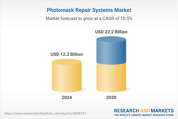
| Estimated Market Value ( USD | $ 12.2 Billion |
| Forecasted Market Value ( USD | $ 22.2 Billion |
| Compound Annual Growth Rate | 10.5% |
| Regions Covered | Global |


