Global Pellicle Market - Key Trends & Drivers Summarized
What Role Do Pellicles Play in Protecting Semiconductor Precision and Photomask Integrity?
Pellicles - thin, transparent membranes affixed to photomasks in semiconductor lithography - serve a critical role in preventing particulate contamination during the photolithography process. These ultra-thin polymer films, usually composed of fluoropolymers, nitrocellulose, or polyimide, act as a physical barrier, ensuring that any particles landing on the pellicle remain out of the mask's focal plane. This safeguard is essential in protecting reticle quality, minimizing defect propagation, and preserving the yield of wafers during high-resolution fabrication processes.As photomask costs increase and critical dimensions shrink below 10 nm, pellicle protection becomes economically and operationally indispensable. Pellicles are especially crucial in deep ultraviolet (DUV) and extreme ultraviolet (EUV) lithography environments, where even nanometer-scale particles can distort circuit patterns. With EUV lithography gaining traction for advanced nodes (5 nm, 3 nm, and beyond), next-generation pellicles must balance high transmission, low reflectivity, extreme heat resistance, and negligible distortion - a challenging feat that's fueling a wave of material and engineering innovations.
How Are EUV Adoption, Wafer Yield Optimization, and Contamination Control Shaping Pellicle Design Evolution?
EUV lithography, operating at a 13.5 nm wavelength, poses unique challenges for pellicle design. Conventional pellicle materials used in DUV lithography absorb too much EUV radiation, compromising throughput. To address this, semiconductor equipment manufacturers and material science firms are developing EUV-compatible pellicles using silicon-based thin films, carbon nanomaterials, and ultra-thin membranes mounted on advanced frames. These EUV pellicles must withstand laser heating, vacuum environments, and high-intensity exposure without degrading image fidelity.Wafer yield remains a cornerstone metric in semiconductor economics, and contamination-induced defects on masks are a direct threat to profitability. As front-end fabs move toward advanced node production, the cost of reprinting defective wafers and the downtime associated with pellicle damage becomes significant. Hence, pellicle designs are now incorporating anti-reflective coatings, frame materials with higher thermal coefficients, and advanced mounting systems that enable easier alignment and lower particle generation.
Why Are Foundry Investments, Material Innovation, and Supply Chain Localization Driving Market Expansion?
Massive capital expenditure by semiconductor foundries - especially in Taiwan, South Korea, Japan, and the U.S. - is fueling demand for high-purity lithographic accessories including pellicles. As governments and chipmakers localize supply chains and reduce dependency on single-country sources, pellicle production is seeing geographic diversification and a shift toward regional sourcing strategies. This is creating opportunities for new players with material science expertise and vacuum manufacturing capabilities to enter the pellicle space.Material innovation is another growth lever. Companies are actively pursuing ultra-thin, defect-free, and high-transmittance pellicle films based on silicon nitride, amorphous carbon, and fluoropolymer composites. Some developers are leveraging atomic layer deposition (ALD) and nanoimprint technologies to achieve pellicles that meet stringent optical, thermal, and mechanical performance specifications for advanced wafer fabs. These breakthroughs are expanding pellicle viability in both DUV and EUV processes.
What's Driving the Global Demand for Pellicles in Semiconductor Manufacturing?
The growth in the pellicle market is driven by several factors including the widespread adoption of EUV lithography, increasing complexity of semiconductor nodes, and growing investments in fab infrastructure worldwide. A primary growth driver is the need for contamination control solutions that ensure consistent wafer yields, minimize downtime, and protect high-cost photomasks in an era of billion-dollar chip fabrication lines.As Moore's Law slows and the cost per node escalates, the role of protective infrastructure such as pellicles becomes more central to maintaining operational efficiency and product reliability. The pellicle market is also expanding through sustained R&D in thermal-resistant materials, low-distortion coatings, and pellicle frame innovations tailored for high-NA EUV tools.
With semiconductor innovation increasingly reliant on sub-nanometer precision and zero-defect execution, pellicles will remain mission-critical components in advanced lithographic ecosystems - supporting global chipmakers in their quest for ever-smaller, faster, and more energy-efficient processors.
Report Scope
The report analyzes the Pellicle market, presented in terms of market value (US$). The analysis covers the key segments and geographic regions outlined below:- Segments: Lithography Technology Type (ArF, EUV, KrF); Application (IC Bumping, IC Foundry, IC Substrate, MEMS, LED Package).
- Geographic Regions/Countries: World; United States; Canada; Japan; China; Europe (France; Germany; Italy; United Kingdom; Spain; Russia; and Rest of Europe); Asia-Pacific (Australia; India; South Korea; and Rest of Asia-Pacific); Latin America (Argentina; Brazil; Mexico; and Rest of Latin America); Middle East (Iran; Israel; Saudi Arabia; United Arab Emirates; and Rest of Middle East); and Africa.
Key Insights:
- Market Growth: Understand the significant growth trajectory of the ArF Lithography Technology segment, which is expected to reach US$676.4 Million by 2030 with a CAGR of a 9.7%. The EUV Lithography Technology segment is also set to grow at 11.4% CAGR over the analysis period.
- Regional Analysis: Gain insights into the U.S. market, valued at $202.2 Million in 2024, and China, forecasted to grow at an impressive 13.8% CAGR to reach $271.4 Million by 2030. Discover growth trends in other key regions, including Japan, Canada, Germany, and the Asia-Pacific.
Why You Should Buy This Report:
- Detailed Market Analysis: Access a thorough analysis of the Global Pellicle Market, covering all major geographic regions and market segments.
- Competitive Insights: Get an overview of the competitive landscape, including the market presence of major players across different geographies.
- Future Trends and Drivers: Understand the key trends and drivers shaping the future of the Global Pellicle Market.
- Actionable Insights: Benefit from actionable insights that can help you identify new revenue opportunities and make strategic business decisions.
Key Questions Answered:
- How is the Global Pellicle Market expected to evolve by 2030?
- What are the main drivers and restraints affecting the market?
- Which market segments will grow the most over the forecast period?
- How will market shares for different regions and segments change by 2030?
- Who are the leading players in the market, and what are their prospects?
Report Features:
- Comprehensive Market Data: Independent analysis of annual sales and market forecasts in US$ Million from 2024 to 2030.
- In-Depth Regional Analysis: Detailed insights into key markets, including the U.S., China, Japan, Canada, Europe, Asia-Pacific, Latin America, Middle East, and Africa.
- Complimentary Updates: Receive free report updates for one year to keep you informed of the latest market developments.
Some of the 34 companies featured in this Pellicle market report include:
- 3M
- AGC Inc.
- ASML Holding N.V.
- Canatu
- Dai Nippon Printing Co., Ltd.
- DuPont
- Entegris, Inc.
- Fine Semitech Corp. (FST)
- Fujifilm Holdings Corporation
- Hitachi Chemical Co., Ltd.
- INKO Industrial Corporation
- Intel Corporation
- JTEKT Corporation
- Micro Lithography Inc.
- Mitsui Chemicals, Inc.
- NEPCO
- SABIC
- Shin-Etsu Chemical Co., Ltd.
- Sumitomo Chemical Co., Ltd.
- Toppan Photomasks, Inc.
This edition integrates the latest global trade and economic shifts into comprehensive market analysis. Key updates include:
- Tariff and Trade Impact: Insights into global tariff negotiations across 180+ countries, with analysis of supply chain turbulence, sourcing disruptions, and geographic realignment. Special focus on 2025 as a pivotal year for trade tensions, including updated perspectives on the Trump-era tariffs.
- Adjusted Forecasts and Analytics: Revised global and regional market forecasts through 2030, incorporating tariff effects, economic uncertainty, and structural changes in globalization. Includes historical analysis from 2015 to 2023.
- Strategic Market Dynamics: Evaluation of revised market prospects, regional outlooks, and key economic indicators such as population and urbanization trends.
- Innovation & Technology Trends: Latest developments in product and process innovation, emerging technologies, and key industry drivers shaping the competitive landscape.
- Competitive Intelligence: Updated global market share estimates for 2025, competitive positioning of major players (Strong/Active/Niche/Trivial), and refined focus on leading global brands and core players.
- Expert Insight & Commentary: Strategic analysis from economists, trade experts, and domain specialists to contextualize market shifts and identify emerging opportunities.
Table of Contents
Companies Mentioned (Partial List)
A selection of companies mentioned in this report includes, but is not limited to:
- 3M
- AGC Inc.
- ASML Holding N.V.
- Canatu
- Dai Nippon Printing Co., Ltd.
- DuPont
- Entegris, Inc.
- Fine Semitech Corp. (FST)
- Fujifilm Holdings Corporation
- Hitachi Chemical Co., Ltd.
- INKO Industrial Corporation
- Intel Corporation
- JTEKT Corporation
- Micro Lithography Inc.
- Mitsui Chemicals, Inc.
- NEPCO
- SABIC
- Shin-Etsu Chemical Co., Ltd.
- Sumitomo Chemical Co., Ltd.
- Toppan Photomasks, Inc.
Table Information
| Report Attribute | Details |
|---|---|
| No. of Pages | 277 |
| Published | February 2026 |
| Forecast Period | 2024 - 2030 |
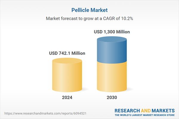
| Estimated Market Value ( USD | $ 742.1 Million |
| Forecasted Market Value ( USD | $ 1300 Million |
| Compound Annual Growth Rate | 10.2% |
| Regions Covered | Global |


