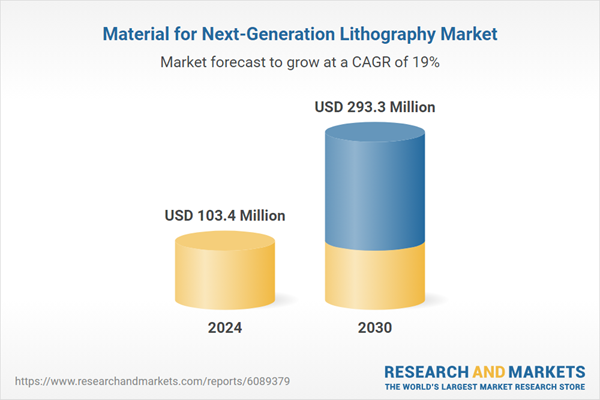
Global Material for Next-Generation Lithography Market - Key Trends & Drivers Summarized
Why Are Specialized Materials Crucial to the Future of Semiconductor Lithography?
Materials for next-generation lithography (NGL) are critical enablers of sub-7nm semiconductor manufacturing technologies, particularly in processes such as extreme ultraviolet (EUV) lithography and directed self-assembly (DSA). As conventional photolithography approaches their physical and optical limits, these advanced materials - comprising resists, underlayers, anti-reflective coatings, and pellicles - ensure precise pattern transfer, line edge roughness control, and high sensitivity at nanoscale dimensions. With demand for more powerful, compact, and energy-efficient chips continuing to rise, next-generation materials are shaping the future of high-performance computing, 5G, AI processors, and advanced memory devices.Unlike earlier nodes that relied heavily on chemically amplified resists for deep ultraviolet (DUV) lithography, NGL processes require materials that can withstand EUV's short 13.5 nm wavelength and high-energy photon bombardment. This demands not only enhanced photoresist chemistries but also improved substrate interfaces, underlayer uniformity, and contamination-free pellicle membranes. These advanced materials ensure pattern fidelity and process reliability, especially as fabs move into high-volume EUV production for logic and DRAM devices.
How Are Material Science Innovations Advancing Lithographic Precision and Efficiency?
Material suppliers are investing heavily in developing novel resist formulations with higher quantum efficiency, low line width roughness (LWR), and excellent etch resistance under EUV exposure. Metal-oxide resists, hybrid organic-inorganic compounds, and low-volume polymer blends are being evaluated to overcome the stochastic effects and resolution challenges introduced at such small feature sizes. These new materials allow for finer pitch scaling and reduce pattern collapse during post-exposure bake and development.Beyond resists, anti-reflective coatings (BARCs) and planarization layers are being optimized for compatibility with EUV optics and pattern transfer requirements. Materials that prevent pattern distortion due to photon scattering and outgassing are essential for mask integrity and yield performance. Pellicles made from ultra-thin, EUV-transparent membranes - such as carbon-based films or silicon nitride composites - are being developed to protect photomasks from particle contamination during exposure. These innovations collectively support higher throughput, lower defect rates, and improved cost-efficiency in EUV lithography.
Which Segments and Applications Are Driving the Need for NGL-Compatible Materials?
The primary demand for next-generation lithography materials originates from advanced semiconductor fabrication, particularly for logic ICs at 5nm, 3nm, and below. Leading foundries and integrated device manufacturers (IDMs) are adopting EUV to produce complex, high-density system-on-chip (SoC) and high-bandwidth memory (HBM) components. Key applications include mobile processors, graphics chips, and AI accelerators, where performance per watt is a competitive differentiator.The DRAM industry is also transitioning toward EUV-based lithography for improved cell scaling and bit density. As back-end packaging techniques like 2.5D and 3D integration become mainstream, material compatibility with heterogeneous chiplets and high aspect-ratio structures becomes essential. Advanced packaging, FOWLP (fan-out wafer-level packaging), and high-density interconnects rely on precision materials that maintain lithographic accuracy across varying topographies. In all these areas, material performance is tightly coupled to overall yield and device functionality.
The Growth in the Material for Next-Generation Lithography Market Is Driven by Several Factors…
The growth in the material for next-generation lithography market is driven by several factors including the rapid miniaturization of semiconductor nodes, accelerated EUV adoption, and increased demand for high-precision patterning in advanced packaging. A key growth driver is the global investment in cutting-edge semiconductor fabs, particularly in Asia, the U.S., and Europe, aimed at securing supply chain resilience and advancing chip design leadership.The need for ultra-sensitive, low-defect resists, advanced pellicles, and EUV-compatible ancillaries is being amplified by rising design complexity in logic and memory chips. Collaborative innovation between fabs, equipment makers, and material suppliers is fostering the development of node-specific chemistries and tailored formulations. Furthermore, regulatory emphasis on sustainability and yield optimization is encouraging the adoption of materials with lower volatility, better recyclability, and minimal outgassing - solidifying their role in next-generation semiconductor manufacturing ecosystems.
Report Scope
The report analyzes the Material for Next-Generation Lithography market, presented in terms of market value (US$). The analysis covers the key segments and geographic regions outlined below:- Segments: Material (Photoresist Material, Ancillary Material); Application (Automotive, Consumer Electronics, IT & Telecommunications, Other Applications).
- Geographic Regions/Countries: World; United States; Canada; Japan; China; Europe (France; Germany; Italy; United Kingdom; Spain; Russia; and Rest of Europe); Asia-Pacific (Australia; India; South Korea; and Rest of Asia-Pacific); Latin America (Argentina; Brazil; Mexico; and Rest of Latin America); Middle East (Iran; Israel; Saudi Arabia; United Arab Emirates; and Rest of Middle East); and Africa.
Key Insights:
- Market Growth: Understand the significant growth trajectory of the Photoresist Material segment, which is expected to reach US$177.8 Million by 2030 with a CAGR of a 17.2%. The Ancillary Material segment is also set to grow at 22% CAGR over the analysis period.
- Regional Analysis: Gain insights into the U.S. market, valued at $28.2 Million in 2024, and China, forecasted to grow at an impressive 24.6% CAGR to reach $65.1 Million by 2030. Discover growth trends in other key regions, including Japan, Canada, Germany, and the Asia-Pacific.
Why You Should Buy This Report:
- Detailed Market Analysis: Access a thorough analysis of the Global Material for Next-Generation Lithography Market, covering all major geographic regions and market segments.
- Competitive Insights: Get an overview of the competitive landscape, including the market presence of major players across different geographies.
- Future Trends and Drivers: Understand the key trends and drivers shaping the future of the Global Material for Next-Generation Lithography Market.
- Actionable Insights: Benefit from actionable insights that can help you identify new revenue opportunities and make strategic business decisions.
Key Questions Answered:
- How is the Global Material for Next-Generation Lithography Market expected to evolve by 2030?
- What are the main drivers and restraints affecting the market?
- Which market segments will grow the most over the forecast period?
- How will market shares for different regions and segments change by 2030?
- Who are the leading players in the market, and what are their prospects?
Report Features:
- Comprehensive Market Data: Independent analysis of annual sales and market forecasts in US$ Million from 2024 to 2030.
- In-Depth Regional Analysis: Detailed insights into key markets, including the U.S., China, Japan, Canada, Europe, Asia-Pacific, Latin America, Middle East, and Africa.
- Company Profiles: Coverage of players such as 3TA Group, Akturk Lojistik Ve Tic. Ltd. Sti., Al Nama Foodstuff Est., Al Nama Herbals, Arizone International LLP and more.
- Complimentary Updates: Receive free report updates for one year to keep you informed of the latest market developments.
Some of the 43 companies featured in this Material for Next-Generation Lithography market report include:
- Allresist GmbH
- Avantor Performance Materials Inc.
- Brewer Science, Inc.
- Carl Zeiss SMT GmbH
- DJ MicroLaminates, Inc.
- Dongjin Semichem Co., Ltd.
- DuPont de Nemours, Inc.
- Fujifilm Corporation
- Irresistible Materials Ltd
- JSR Corporation
- Kayaku Advanced Materials, Inc.
- KemLab Inc.
- Merck KGaA
- micro resist technology GmbH
- SACHEM, Inc.
- Shin-Etsu Chemical Co., Ltd.
- Sumitomo Chemical Co., Ltd.
- Tokyo Ohka Kogyo Co., Ltd. (TOK)
- Weifang Startech Microelectronic Materials Co., Ltd.
- Zeon Corporation
This edition integrates the latest global trade and economic shifts into comprehensive market analysis. Key updates include:
- Tariff and Trade Impact: Insights into global tariff negotiations across 180+ countries, with analysis of supply chain turbulence, sourcing disruptions, and geographic realignment. Special focus on 2025 as a pivotal year for trade tensions, including updated perspectives on the Trump-era tariffs.
- Adjusted Forecasts and Analytics: Revised global and regional market forecasts through 2030, incorporating tariff effects, economic uncertainty, and structural changes in globalization. Includes historical analysis from 2015 to 2023.
- Strategic Market Dynamics: Evaluation of revised market prospects, regional outlooks, and key economic indicators such as population and urbanization trends.
- Innovation & Technology Trends: Latest developments in product and process innovation, emerging technologies, and key industry drivers shaping the competitive landscape.
- Competitive Intelligence: Updated global market share estimates for 2025, competitive positioning of major players (Strong/Active/Niche/Trivial), and refined focus on leading global brands and core players.
- Expert Insight & Commentary: Strategic analysis from economists, trade experts, and domain specialists to contextualize market shifts and identify emerging opportunities.
Table of Contents
Companies Mentioned (Partial List)
A selection of companies mentioned in this report includes, but is not limited to:
- Allresist GmbH
- Avantor Performance Materials Inc.
- Brewer Science, Inc.
- Carl Zeiss SMT GmbH
- DJ MicroLaminates, Inc.
- Dongjin Semichem Co., Ltd.
- DuPont de Nemours, Inc.
- Fujifilm Corporation
- Irresistible Materials Ltd
- JSR Corporation
- Kayaku Advanced Materials, Inc.
- KemLab Inc.
- Merck KGaA
- micro resist technology GmbH
- SACHEM, Inc.
- Shin-Etsu Chemical Co., Ltd.
- Sumitomo Chemical Co., Ltd.
- Tokyo Ohka Kogyo Co., Ltd. (TOK)
- Weifang Startech Microelectronic Materials Co., Ltd.
- Zeon Corporation
Table Information
| Report Attribute | Details |
|---|---|
| No. of Pages | 280 |
| Published | January 2026 |
| Forecast Period | 2024 - 2030 |
| Estimated Market Value ( USD | $ 103.4 Million |
| Forecasted Market Value ( USD | $ 293.3 Million |
| Compound Annual Growth Rate | 19.0% |
| Regions Covered | Global |


